Difference between revisions of "Recore A6"
(→A64) |
(→A64) |
||
| Line 33: | Line 33: | ||
{| class="wikitable" | {| class="wikitable" | ||
| − | ! | + | !Name |
| − | + | !Bank and pin | |
| − | + | !style="border-right:solid 2px;"| Number | |
| − | + | !Name | |
| − | |Number | + | !Bank and pin |
| − | + | !style="border-right:solid 2px;"| Number | |
| − | + | !Name | |
| − | |Number | + | !Bank and pin |
| − | + | !Number | |
| − | |||
| − | |||
|- | |- | ||
|END STOP 0 | |END STOP 0 | ||
|PH4 | |PH4 | ||
| − | |228 | + | |style="border-right:solid 2px;"|228 |
|DIR 6 | |DIR 6 | ||
|PE14 | |PE14 | ||
| − | |142 | + | |style="border-right:solid 2px;"|142 |
|USB-PWR-EN-0 | |USB-PWR-EN-0 | ||
|PH0 | |PH0 | ||
| Line 57: | Line 55: | ||
|END STOP 1 | |END STOP 1 | ||
|PH5 | |PH5 | ||
| − | |229 | + | |style="border-right:solid 2px;"|229 |
|DIR 7 | |DIR 7 | ||
|PE15 | |PE15 | ||
| − | |143 | + | |style="border-right:solid 2px;"|143 |
|USB-PWR-EN-1 | |USB-PWR-EN-1 | ||
|PH1 | |PH1 | ||
| Line 67: | Line 65: | ||
|END STOP 2 | |END STOP 2 | ||
|PH6 | |PH6 | ||
| − | |230 | + | |style="border-right:solid 2px;"|230 |
|STEP DIAG 0 | |STEP DIAG 0 | ||
|PE0 | |PE0 | ||
| − | |128 | + | |style="border-right:solid 2px;"|128 |
|USB-PWR-EN-2 | |USB-PWR-EN-2 | ||
|PH2 | |PH2 | ||
| Line 77: | Line 75: | ||
|END STOP 3 | |END STOP 3 | ||
|PH7 | |PH7 | ||
| − | |231 | + | |style="border-right:solid 2px;"|231 |
|STEP DIAG 1 | |STEP DIAG 1 | ||
|PE1 | |PE1 | ||
| − | |129 | + | |style="border-right:solid 2px;"|129 |
|USB-PWR-EN-3 | |USB-PWR-EN-3 | ||
|PH3 | |PH3 | ||
| Line 87: | Line 85: | ||
|END STOP 4 | |END STOP 4 | ||
|PH8 | |PH8 | ||
| − | |232 | + | |style="border-right:solid 2px;"|232 |
|STEP DIAG 2 | |STEP DIAG 2 | ||
|PE2 | |PE2 | ||
| − | |130 | + | |style="border-right:solid 2px;"|130 |
|GAIN-ENABLE-T0 | |GAIN-ENABLE-T0 | ||
|PD4 | |PD4 | ||
| Line 97: | Line 95: | ||
|END STOP 5 | |END STOP 5 | ||
|PH9 | |PH9 | ||
| − | |233 | + | |style="border-right:solid 2px;"|233 |
|STEP DIAG 3 | |STEP DIAG 3 | ||
|PE3 | |PE3 | ||
| − | |131 | + | |style="border-right:solid 2px;"|131 |
|GAIN-ENABLE-T1 | |GAIN-ENABLE-T1 | ||
|PH11 | |PH11 | ||
| Line 107: | Line 105: | ||
|STEP 0 | |STEP 0 | ||
|PL4 | |PL4 | ||
| − | |4 | + | |style="border-right:solid 2px;"|4 |
|STEP DIAG 4 | |STEP DIAG 4 | ||
|PE4 | |PE4 | ||
| − | |132 | + | |style="border-right:solid 2px;"|132 |
|GAIN ENABLE T2 | |GAIN ENABLE T2 | ||
|PE17 | |PE17 | ||
| Line 117: | Line 115: | ||
|STEP 1 | |STEP 1 | ||
|PL5 | |PL5 | ||
| − | |5 | + | |style="border-right:solid 2px;"|5 |
|STEP DIAG 5 | |STEP DIAG 5 | ||
|PE5 | |PE5 | ||
| − | |133 | + | |style="border-right:solid 2px;"|133 |
|GAIN ENABLE T3 | |GAIN ENABLE T3 | ||
|PB2 | |PB2 | ||
| Line 127: | Line 125: | ||
|STEP 2 | |STEP 2 | ||
|PL6 | |PL6 | ||
| − | |6 | + | |style="border-right:solid 2px;"|6 |
|STEP DIAG 6 | |STEP DIAG 6 | ||
|PE6 | |PE6 | ||
| − | |134 | + | |style="border-right:solid 2px;"|134 |
|PU-ENABLE-T0 | |PU-ENABLE-T0 | ||
|PG10 | |PG10 | ||
| Line 137: | Line 135: | ||
|STEP 3 | |STEP 3 | ||
|PL7 | |PL7 | ||
| − | |7 | + | |style="border-right:solid 2px;"|7 |
|STEP DIAG 7 | |STEP DIAG 7 | ||
|PE7 | |PE7 | ||
| − | |135 | + | |style="border-right:solid 2px;"|135 |
|PU-ENABLE-T1 | |PU-ENABLE-T1 | ||
|PG11 | |PG11 | ||
| Line 147: | Line 145: | ||
|STEP 4 | |STEP 4 | ||
|PL8 | |PL8 | ||
| − | |8 | + | |style="border-right:solid 2px;"|8 |
|OC-ALERT | |OC-ALERT | ||
|PF6 | |PF6 | ||
| − | |166 | + | |style="border-right:solid 2px;"|166 |
|PU ENABLE T2 | |PU ENABLE T2 | ||
|PG12 | |PG12 | ||
| Line 157: | Line 155: | ||
|STEP 5 | |STEP 5 | ||
|PL9 | |PL9 | ||
| − | |9 | + | |style="border-right:solid 2px;"|9 |
|OC-RESET | |OC-RESET | ||
|PF4 | |PF4 | ||
| − | |164 | + | |style="border-right:solid 2px;"|164 |
|PU ENABLE T3 | |PU ENABLE T3 | ||
|PG13 | |PG13 | ||
| Line 167: | Line 165: | ||
|STEP 6 | |STEP 6 | ||
|PL10 | |PL10 | ||
| − | |10 | + | |style="border-right:solid 2px;"|10 |
|EN-HP | |EN-HP | ||
|PF5 | |PF5 | ||
| − | |165 | + | |style="border-right:solid 2px;"|165 |
|OFFSET-T0 | |OFFSET-T0 | ||
|PG0 | |PG0 | ||
| Line 177: | Line 175: | ||
|STEP 7 | |STEP 7 | ||
|PL11 | |PL11 | ||
| − | |11 | + | |style="border-right:solid 2px;"|11 |
|UC-INT-1 | |UC-INT-1 | ||
|PG3 | |PG3 | ||
| − | |195 | + | |style="border-right:solid 2px;"|195 |
|OFFSET-T1 | |OFFSET-T1 | ||
|PG1 | |PG1 | ||
| Line 187: | Line 185: | ||
|DIR 0 | |DIR 0 | ||
|PE8 | |PE8 | ||
| − | |136 | + | |style="border-right:solid 2px;"|136 |
|UC-NRST | |UC-NRST | ||
|PG4 | |PG4 | ||
| − | |196 | + | |style="border-right:solid 2px;"|196 |
|OFFSET-T2 | |OFFSET-T2 | ||
|PG3 | |PG3 | ||
| Line 197: | Line 195: | ||
|DIR 1 | |DIR 1 | ||
|PE9 | |PE9 | ||
| − | |137 | + | |style="border-right:solid 2px;"|137 |
|UC-BOOT | |UC-BOOT | ||
|PG5 | |PG5 | ||
| − | |197 | + | |style="border-right:solid 2px;"|197 |
|OFFSET-T3 | |OFFSET-T3 | ||
|PG8 | |PG8 | ||
| Line 207: | Line 205: | ||
|DIR 2 | |DIR 2 | ||
|PE10 | |PE10 | ||
| − | |138 | + | |style="border-right:solid 2px;"|138 |
|ES-EN-12V | |ES-EN-12V | ||
|PF0 | |PF0 | ||
| − | |160 | + | |style="border-right:solid 2px;"|160 |
|STEPPER UART 2 TX | |STEPPER UART 2 TX | ||
|PB0 | |PB0 | ||
| Line 217: | Line 215: | ||
|DIR 3 | |DIR 3 | ||
|PE11 | |PE11 | ||
| − | |139 | + | |style="border-right:solid 2px;"|139 |
|EN-HDMI-PWR | |EN-HDMI-PWR | ||
|PG9 | |PG9 | ||
| − | |201 | + | |style="border-right:solid 2px;"|201 |
|STEPPER UART 2 RX | |STEPPER UART 2 RX | ||
|PB1 | |PB1 | ||
| Line 227: | Line 225: | ||
|DIR 4 | |DIR 4 | ||
|PE12 | |PE12 | ||
| − | |140 | + | |style="border-right:solid 2px;"|140 |
|EN-THERMISTORS | |EN-THERMISTORS | ||
|PF1 | |PF1 | ||
| − | |161 | + | |style="border-right:solid 2px;"|161 |
|STEPPER UART 3 TX | |STEPPER UART 3 TX | ||
|PD0 | |PD0 | ||
| Line 237: | Line 235: | ||
|DIR 5 | |DIR 5 | ||
|PE13 | |PE13 | ||
| − | |141 | + | |style="border-right:solid 2px;"|141 |
|EN-ENDSTOPS | |EN-ENDSTOPS | ||
|PF2 | |PF2 | ||
| − | |162 | + | |style="border-right:solid 2px;"|162 |
|STEPPER UART 3 RX | |STEPPER UART 3 RX | ||
|PD1 | |PD1 | ||
Revision as of 18:24, 20 January 2022
Contents
- 1 Recore Rev A6
- 2 Hardware overview
- 3 Connectors
- 4 BLtouch
- 5 Current limits
- 6 Temperature inputs
- 7 Software for Recore
- 8 Manual control and testing
- 9 Performance
- 10 FAQ
- 10.1 Q: Where can I ask for help?
- 10.2 Q: What comes in the box with the Recore? Specifically, terminal connectors for power, etc?
- 10.3 Q: What's the maximum current draw for heat bed?
- 10.4 Q Why are there unused and unbroken out pins on the STM32 MCU?
- 10.5 Q: I have a gadget that I want to connect with SPI. Is that possible?
- 10.6 Q: What exactly is the role of the AR100 device?
- 10.7 Q: What voltage fans are supported?
- 10.8 Q: Where is the board layout file?
- 10.9 Q: Where are you shipping from?
- 11 Known Issues
Recore Rev A6
 Recore is a 3D-printer control board running Linux. It is specifically tailored to be compatible with Klipper and OctoPrint. The main features are:
- Allwinner A64 SoC, quad core CPU running at 1 GHz.
- 1 GB or DDR3 RAM
- 8 GB of on board eMMC
- Gigabit Ethernet
- 6 TMC2209, 2 A stepper motor drivers
- 3 heater outputs + high power heated bed
- 4 USB High Speed ports
- 4 thermistor/thermocouple inputs (software selectable)
- Comes with Debian Linux with Klipper and OctoPrint installed
This document is for Recore Revision A5. For previous hardware revisions, please see:
Hardware overview
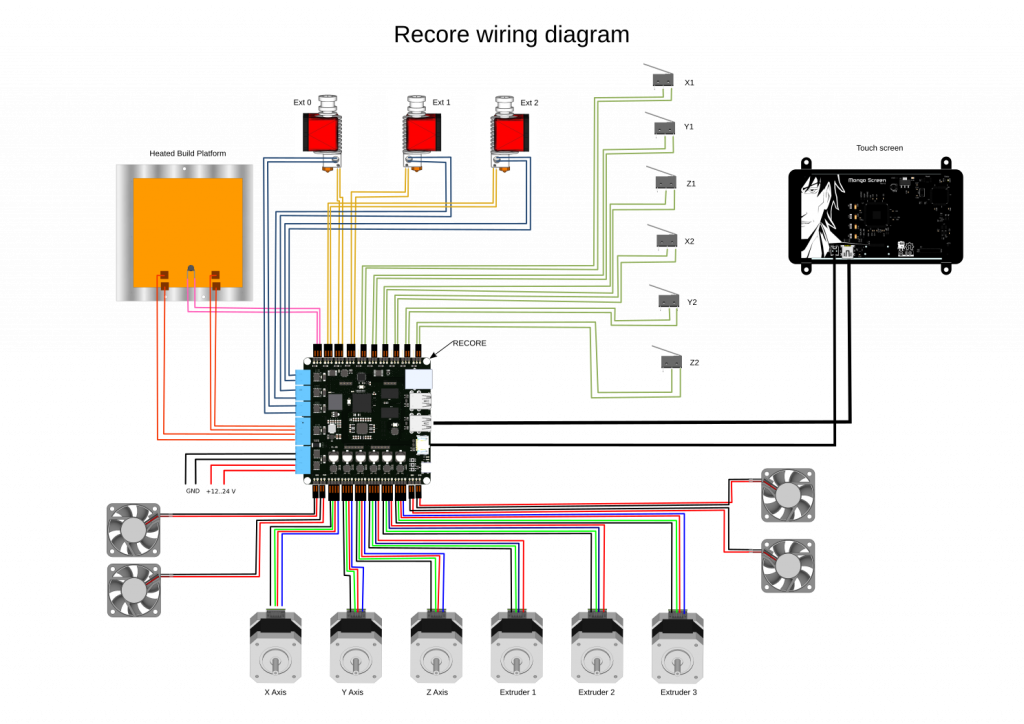
Wiring diagram
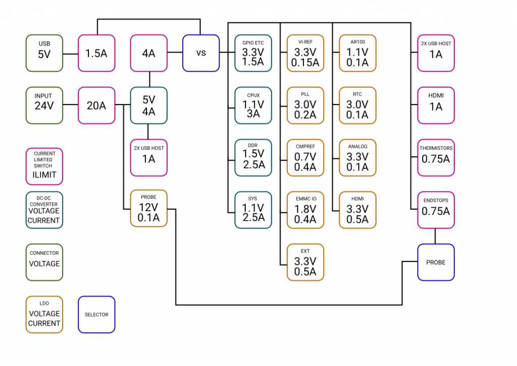
Power domain overview
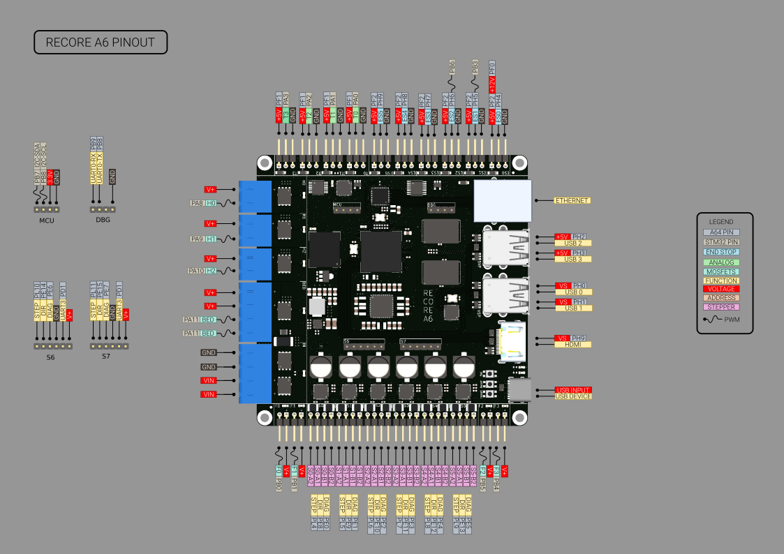
Pinout
A64
In the following table the pins used for End-stops and stepper control are described. The "bank and pin" can be used to specify the pin numbers in klipper. The "Number" column is useful for testing things on the command line in conjunction with gpiod.
| Name | Bank and pin | Number | Name | Bank and pin | Number | Name | Bank and pin | Number |
|---|---|---|---|---|---|---|---|---|
| END STOP 0 | PH4 | 228 | DIR 6 | PE14 | 142 | USB-PWR-EN-0 | PH0 | 224 |
| END STOP 1 | PH5 | 229 | DIR 7 | PE15 | 143 | USB-PWR-EN-1 | PH1 | 225 |
| END STOP 2 | PH6 | 230 | STEP DIAG 0 | PE0 | 128 | USB-PWR-EN-2 | PH2 | 226 |
| END STOP 3 | PH7 | 231 | STEP DIAG 1 | PE1 | 129 | USB-PWR-EN-3 | PH3 | 227 |
| END STOP 4 | PH8 | 232 | STEP DIAG 2 | PE2 | 130 | GAIN-ENABLE-T0 | PD4 | 100 |
| END STOP 5 | PH9 | 233 | STEP DIAG 3 | PE3 | 131 | GAIN-ENABLE-T1 | PH11 | 235 |
| STEP 0 | PL4 | 4 | STEP DIAG 4 | PE4 | 132 | GAIN ENABLE T2 | PE17 | 145 |
| STEP 1 | PL5 | 5 | STEP DIAG 5 | PE5 | 133 | GAIN ENABLE T3 | PB2 | 34 |
| STEP 2 | PL6 | 6 | STEP DIAG 6 | PE6 | 134 | PU-ENABLE-T0 | PG10 | 202 |
| STEP 3 | PL7 | 7 | STEP DIAG 7 | PE7 | 135 | PU-ENABLE-T1 | PG11 | 203 |
| STEP 4 | PL8 | 8 | OC-ALERT | PF6 | 166 | PU ENABLE T2 | PG12 | 204 |
| STEP 5 | PL9 | 9 | OC-RESET | PF4 | 164 | PU ENABLE T3 | PG13 | 205 |
| STEP 6 | PL10 | 10 | EN-HP | PF5 | 165 | OFFSET-T0 | PG0 | 192 |
| STEP 7 | PL11 | 11 | UC-INT-1 | PG3 | 195 | OFFSET-T1 | PG1 | 193 |
| DIR 0 | PE8 | 136 | UC-NRST | PG4 | 196 | OFFSET-T2 | PG3 | 194 |
| DIR 1 | PE9 | 137 | UC-BOOT | PG5 | 197 | OFFSET-T3 | PG8 | 200 |
| DIR 2 | PE10 | 138 | ES-EN-12V | PF0 | 160 | STEPPER UART 2 TX | PB0 | 32 |
| DIR 3 | PE11 | 139 | EN-HDMI-PWR | PG9 | 201 | STEPPER UART 2 RX | PB1 | 33 |
| DIR 4 | PE12 | 140 | EN-THERMISTORS | PF1 | 161 | STEPPER UART 3 TX | PD0 | 96 |
| DIR 5 | PE13 | 141 | EN-ENDSTOPS | PF2 | 162 | STEPPER UART 3 RX | PD1 | 97 |
STM32F031
| Pinout | ||
|---|---|---|
| Name | Bank and pin | Number |
| THERMISTOR 0 | PA0 | 6 |
| THERMISTOR 1 | PA1 | 7 |
| THERMISTOR 2 | PA2 | 8 |
| THERMISTOR 3 | PA3 | 9 |
| BOARD VOLTAGE | PA4 | 10 |
| BOARD CURRENT | PA5 | 11 |
| BOARD TEMPERATURE | PA6 | 12 |
| COLD JUNCTION | PA7 | 13 |
| FAN 0 | PB0 | 14 |
| FAN 1 | PB1 | 15 |
| FAN 2 | PB5 | 28 |
| FAN 3 | PB4 | 27 |
| HEATER E0 | PA8 | 18 |
| HEATER E1 | PA9 | 19 |
| HEATER E2 | PA10 | 20 |
| HEATER BED | PA11 | 21 |
| USER LED | PA12 | 22 |
| EXT 1 | PB8 | 32 |
| EXT 2 | PB7 | 30 |
Inductive Sensor
Connect the inductive sensor on ES0. You can choose either 5V or 12V output on the voltage pin.
| Pinout | |
|---|---|
| Name | Number |
| Black | signal |
| Blue | GND |
| Brown | 12V |
DBG header
This header is used for interacting with u-boot and getting early debug messages from the Linux kernel
| Pinout | |
|---|---|
| Pin | Function |
| 1 | UART RX |
| 2 | UART TX |
| 3 | NC |
| 4 | GND |
MCU header
This header is used for connecting additional MCU peripherals.
| Pinout | ||
|---|---|---|
| Pin | Function | Alt |
| 1 | PB7 | I2C1_SDA |
| 2 | PB8 | I2C1_SCL |
| 3 | 3.3V | |
| 4 | GND | |
LEDs
There are 15 white LEDs on the board. Here is what they mean
| LEDS meaning | ||
|---|---|---|
| Name | Location | Meaning |
| D2 | By PMIC | Board powered |
| D3 | By heater BED | BED output on |
| D4 | By fan 0 | Fan 0 is on |
| D5 | By fan 1 | Fan 1 is on |
| D6 | By heater H2 | Heater H1 is on |
| D7 | By fan 2 | Fan 2 is on |
| D8 | By heater H0 | Heater H0 is on |
| D9 | By fan 3 | Fan 3 is on |
| D10 | By heater H1 | Heater H1 is on |
| D12 | By input connector | High voltage domain is on |
| D15 | By eMMC chip | eMMC activity |
| D17 | By HDMI connector | Reserved |
| D18 | By the USB C connector | Linux Heartbeat |
| D19 | By the A64 SoC | CPU activity |
| D20 | By the STM32 | Klipper running on STM32 |
Connectors
The power connectors on the board are available either in the web shop as part of a connector pack or directly from Digi-key etc.
Four pin male: TBP01P1-508-04BE [| Digi-key]
Two pin male: TBP01P1-508-02BE [| Digi-key]
TMC2209
The 6 stepper drivers on Recore are of type TMC2209 from Trinamic. Each stepper has a configuration interface with a bidirectional UART port that is connected to a peripheral UART on the A64. The peripheral is not in use, but instead the GPIO bit-banging functionality of Klipper is used to communicate with the stepper drivers.
Due to space constraints, the TMC2209s use internal sense resistors for measuring current in a constant current setup. The R_REF as specified in the TMC2209 datasheet is a 6.8K resistor giving a maximum peak current of 1.92 A, RMS current of 1.35 A.
Here is a table with pins and addresses for the steppers
| Stepper driver config | ||
|---|---|---|
| Name | Pins | Address |
| S0 | PB0/PB1 | 0 |
| S1 | PB0/PB1 | 1 |
| S2 | PB0/PB1 | 2 |
| S3 | PB0/PB1 | 3 |
| S4 | PD0/PD1 | 0 |
| S5 | PD0/PD1 | 1 |
| S6 | PD0/PD1 | 2 |
| S7 | PD0/PD1 | 3 |
BLtouch
Setting up BLtouch can be done by using the following section
[bltouch]
sensor_pin: ^ar100:PH7
control_pin: PB7
speed: 7
pin_move_time: 0.675
sample_retract_dist: 10
pin_up_reports_not_triggered: True
pin_up_touch_mode_reports_triggered: True
z_offset: 2.22
x_offset: -28
y_offset: -13
Current limits
| Current limit | |
|---|---|
| Name | Limit |
| 5V-ES | 1 A |
| USB host each | 1 A |
| Thermistors | 1 A |
| MCU connector | 1.5 A (shared with other things) |
Temperature inputs
4 different temperature devices can be connected to the 4 analog inputs on Recore. Thermistor, Thermocouple, PT100 with INA826 and PT1000 without the use of a pre-amplifier.
Thermistor
Make sure the pull-up is enabled and the op-amp gain is set to 1.
Thermocouple
Make sure the pull-up is disabled and the op-amp gain is set to 100.
PT100 with INA826
In order to use a PT100 sensor, an external amplifier board must be used. There is an example configuration for Klipper that uses this. The ADC reference voltage is 5.0 by default, but for Recore it is 3.3 V. Here is an example:
[Extruder]
...
sensor_type: PT100 INA826
adc_voltage: 3.27
The pull-up must also be disabled.
PT1000
Make sure the pull-up is enabled and the gain is set to 1. In the latest version, the sensor must be prefixed with RECORE.
[Extruder]
...
sensor_type: RECORE PT1000
adc_voltage: 3.27
pullup_voltage: 3.3
offset_voltage: 3.2
Software for Recore
Recore comes with the Linux distro Refactor (Armbian) pre-installed on the eMMC. For more instructions about software for Recore, see the Refactor wiki page: Refactor#Recore
AR100
Please see: AR100
Manual control and testing
Power domains
There are 9 power domains around the board controlling voltage on different pins:
- Input power controls power to 4 high power outputs, the 4 fans and the 6 stepper drivers. This input has current monitoring, fast acting over current protection, voltage monitoring, temperature monitoring and reverse polarity protection.
- Thermo couple power Controls +5V/1A output to the ADCs. This can be used for turning on power to the analog pins.
- End stop power Controls +5V/1A output on the six endstops. Ganged. ES5 can be switched to have 12V output. The 12V output has a
100mA internal current limit.
- 4 USB host power domains Controls 5V/1A current output to the usb host connectors. These are turned on by u-boot.
- HDMI 5V output Controls the 5V/1A HDMI output. Turned on by u-boot.
Input stage
Reset over current protection and set it in "one-shot" mode.
gpioset 1 164=0
gpioset 1 164=1
The over current protection can also be set in "transparent" mode, where the current alarm will be reset automatically. Note that this is a bad idea for general operation, only use for testing.
gpioset 1 164=0
Enable 24V input
gpioset 1 165=0
End stop 5V /12V
End stop 0 to 4 has a programmable +5V output voltage. End stop 5 has +5V or +12V selectable.
To enable +5V on ES 0...4
gpioset 1 162=1
To disable again
gpioset 1 162=0
To switch to 12V output on ES5
gpioset 1 160=1
To disable again
gpioset 1 160=0
End stops values
To see what value the end stops have
gpioget 1 228 # ES 5
gpioget 1 229
gpioget 1 230
gpioget 1 231
gpioget 1 232
gpioget 1 233 # ES 0
TMC2209
In window/shell 1:
stty -F /dev/ttyS2 raw -echoe -echo
xxd -c 4 /dev/ttyS2
In window/shell 2:
echo -n -e '\x5\x0\x6\x6F' > /dev/ttyS2
The return should be along the lines of
00000000: 0500 066f  ...o
00000004: 05ff 0620  ...
00000008: 0001 4058  ..@X
To read the OTP registers
echo -n -e "\x5\x0\x5\x21" > /dev/ttyS2
echo -n -e "\x5\x0\x5\x21" > /dev/ttyS3
echo -n -e "\x5\x1\x5\x97" > /dev/ttyS2
echo -n -e "\x5\x1\x5\x97" > /dev/ttyS3
echo -n -e "\x5\x2\x5\x7a" > /dev/ttyS2
echo -n -e "\x5\x2\x5\x7a" > /dev/ttyS3
echo -n -e "\x5\x3\x5\xcc" > /dev/ttyS2
echo -n -e "\x5\x3\x5\xcc" > /dev/ttyS3
To set the OTP register to use RDSon:
echo -n -e "\x5\x0\x84\x0\x0\xbd\x6\xac" > /dev/ttyS2
To check that no errors are reported by the steppers write this on the command line. If a "1" shows up, that is an indication that the motor is reporting an error.
gpioget 1 128
gpioget 1 129
gpioget 1 130
gpioget 1 131
gpioget 1 132
gpioget 1 133
STM32F031
There is a small firmware to test all functionality that is controlled by the STM32F031 chip on the board. Once uploaded to the board using the flash script, the firmware will turn on all LEDs it controls and send back ADC readings.
To flash this firmware to the STM32:
gpioset 1 197=1
gpioset 1 196=0
stm32flash -i -196,196 -w Sumato-f031.bin -v -g 0x00 /dev/ttyS1
gpioset 1 197=0
stm32flash -i -196,196 /dev/ttyS1
To see the ADC readings:
stty -F /dev/ttyS3 38400 raw
cat /dev/ttyS3
You should see something like
ADC T0: 0
ADC T1: 0
ADC T2: 0
ADC T3: 0
ADC U: 2338
ADC I: 0
ADC TB: 3417
The following one-liners assumes gawk is installed.
Reading Current
There is board current reading implemented in OctoPrint. The current shunt resistor is 1 mOhm, the amplifier is 20 times, the vref is 3.3V, so we get: (adc_val/4096*3.3)*1000/20 = (adc_val/4096)*165
If the testing firmware is installed on the STM32, you can convert the current (as in amps) reading to something useful like this:
cat /dev/ttyS4 | awk '/I:/ { printf "scale=4; (%i/4096)*165\n", $3; fflush(); }' | bc -l
Current limit programming
The current limit must be set in the device tree by programming the voltage on dldo2. dldo2 can have values from 0.7 V to 3.4 V. Setting the voltage level to 3.4 V effectively disables the fast acting current limit. Setting it to the lowest value gives an over current limit of 35 A.
Reading Board Temperature
To see the temperature readings, try this :
export beta=4327
cat /dev/ttyS1 | awk '/TB:/ { printf "scale=4; 4327/l( (4700/((3.3/(3.3*%i/4096))-1.0))/0.05306820342563400000) -273.15\n", $3; fflush(); }' | bc -l | awk '{print strftime("%k:%M:%S"), $0; fflush();}'
Reading Input Voltage
To see voltage on the input, it can be converted like this:
exec 4</dev/ttyS4 5>/dev/ttyS4
echo -n ";A4;" >&5
read -t1 reply <&4
echo $reply | awk '{ printf "scale=4; (%i/4096)*3.3*((100+10)/10)\n", $4; fflush(); }' | bc -l
Thermistor inputs
To enable pull-up on input for using thermistors for temperature measurements:
gpioset 1 102=1
gpioset 1 120=1
gpioset 1 160=1
gpioset 1 161=1
Setting Op-amp gain to 1:
gpioget 1 100
gpioget 1 235
gpioget 1 145
gpioget 1 34
In the device tree file, the gpio/ldos must be set to gpio input:
&gpio0_ldo {
  function = "gpio_in";
};
Thermocouple input
Either a thermocouple or a thermistor can be used as input on the T0-T3 inputs.
Bias
The thermocouple is set up to have a Bias of 0.7V/100 on the input which enables negative values (lower than the board temperature) as input to the ADCs. With the input short circuited, the bias can be recorded. Typical values are 750 This needs to be subtracted from the result.
Cold junction compensation
Another important aspect is cold junction compensation. There is a thermistor connected on the board close to the thermocouple inputs which can be used to measure the temperature close to the input junction. This temperature must be added in software.
The connected thermistor is a TDK NTCG104EF104FT1X The connected Thermocouple has a (25/100) beta value of 4327.
In order to use the inputs for thermocouple, the pull-up-down resistors must be set to pull-down:
gpioset 1 102=0
gpioset 1 120=0
gpioset 1 160=0
gpioset 1 161=0
Also, the op-amp needs a gain of 100:
gpioset 1 100=0
gpioset 1 235=0
gpioset 1 145=0
gpioset 1 34=0
Finally, the input bias needs to be enabled. The following LDOs needs to be enabled:
reg_ldo_io0
reg_ldo_io1
reg_dldo3
reg_dldo4
Performance
Start-up time
With a maximum clock for MMC2 of 200 MHz, here is the start-up time:
root@recore-3:~# systemd-analyze
Startup finished in 5.128s (kernel) + 11.567s (userspace) = 16.695s
graphical.target reached after 11.421s in userspace
Measured voltages
Instruments used:
- Siglent SDM3065X, 6.5 digit multimeter
- HP 3458A, 8.5 digit multimeter
- HP 3245A, Universal Source
Microcontroller voltages
VDDA uC: 3.312 V
VDD uC: 3.312 V
Voltage from the PMIC supplied as bias:
0.706 V
Offset and Gain Measurements
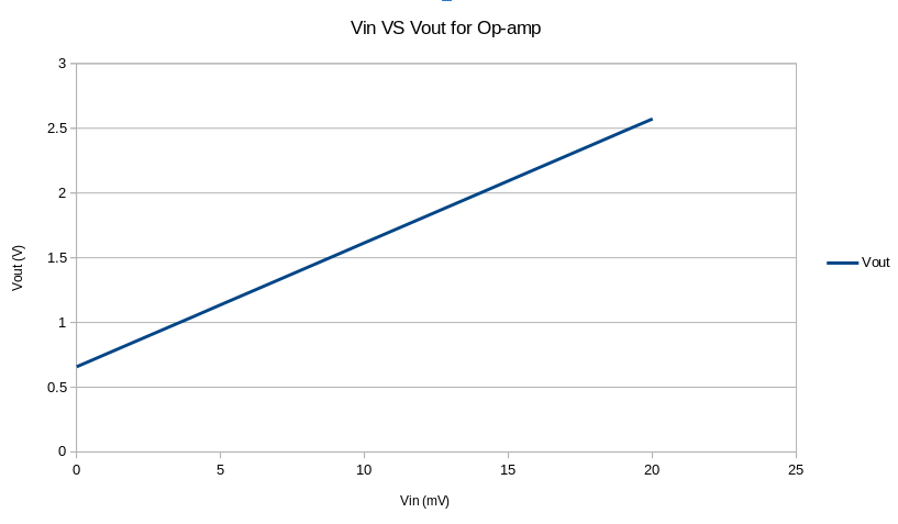
Input voltage measured with SDM3065X, output voltage measured with 3458A. Programmable Voltage reference used was the DIY DAC cape made by Elias. Measurements should be repeated with HP 3245A.
| Op-amp gain measurements | ||
|---|---|---|
| Vin (mV) | Vout (V) | Gain |
| 1.0103 | 0.754 | 95.73 |
| 2.0038 | 0.8492 | 95.78 |
| 3.013 | 0.9457 | 95.72 |
| 4.0032 | 1.04 | 95.60 |
| 5.0108 | 1.1372 | 95.78 |
| 6.0016 | 1.232 | 95.76 |
| 7.0094 | 1.3285 | 95.76 |
| 8.0015 | 1.4235 | 95.76 |
| 9.0106 | 1.5201 | 95.76 |
| 10.0005 | 1.615 | 95.77 |
| 11.0102 | 1.7116 | 95.76 |
| 12.0042 | 1.8067 | 95.75 |
| 13.0142 | 1.9035 | 95.76 |
| 14.0056 | 1.9985 | 95.76 |
| 15.0145 | 2.095 | 95.76 |
| 16.0055 | 2.1899 | 95.76 |
| 17.0145 | 2.2865 | 95.75 |
| 18.0055 | 2.3813 | 95.75 |
| 19.0163 | 2.4783 | 95.76 |
| 20.0067 | 2.5723 | 95.72 |
An experiment was done using an HP 3245A and a HP 3458A measuring the input and output voltages and calculating offset and gain. This will become a part of a calibration routine during final testing and flashing, values should be stored with the board.
Input 1	Vin	Vout	Offset
	0.0003	0.6685	0.6685

Vin set	Vin	Vout	Gain	Deviation
-5 mV	-4.9983	0.1840	96.93	0.16
0 mV	0.0003	0.6685	96.76	-0.01
5 mV	5.0000	1.1523	96.77	0.00
10 mV	10.0013	1.6355	96.69	-0.08
15 mV	15.0005	2.1198	96.75	-0.01
20 mV	20.0005	2.6025	96.70	-0.07
	Average gain		96.77


Input 2	Vin	Vout	Offset
	0.0017	0.6485	0.6483


Vin set	Vin	Vout	Gain	Deviation
-5 mV	-4.9961	0.1722	95.30	-0.07
0 mV	0.0017	0.6485	95.37	-0.01
5 mV	5.0014	1.1253	95.37	-0.01
10 mV	10.003	1.6025	95.39	0.01
15 mV	15.0021	2.0793	95.38	0.01
20 mV	20.0023	2.5559	95.37	-0.01
	Average gain		95.38


Input 3	Vin	Vout	Offset
	0.0013	0.6560	0.6559


Vin set	Vin	Vout	Gain	Deviation
-5 mV	-4.9969	0.1794	95.35	-0.02
0 mV	0.0013	0.6560	95.35	-0.03
5 mV	5.0012	1.1329	95.38	0.01
10 mV	10.0025	1.6098	95.37	-0.01
15 mV	15.0015	2.0864	95.36	-0.02
20 mV	20.0013	2.5631	95.35	-0.02
	Average gain		95.36


Input 4	Vin	Vout	Offset
	0.0024	0.6498	0.6496


Vin set	Vin	Vout	Gain	Deviation
-5 mV	-4.9954	0.1714	96.98	1.18
0 mV	0.0024	0.6498	94.50	-1.31
5 mV	5.0015	1.1283	95.96	0.16
10 mV	10.0028	1.6069	95.83	0.02
15 mV	15.0024	2.0853	95.78	-0.02
20 mV	20.0022	2.5642	95.78	-0.02
	Average gain		95.81
5V Buck converter ripple and noise
The 5V step down/Buck converter is a AOZ2151PQI-10. It can provide 4A and has an input voltage range of 12-28V. It is hard wired to be in PWM mode. PFM mode results in a loud whine.
Below is a screenshot of the ripple and noise across the the 5V rail with a normal kernel running. 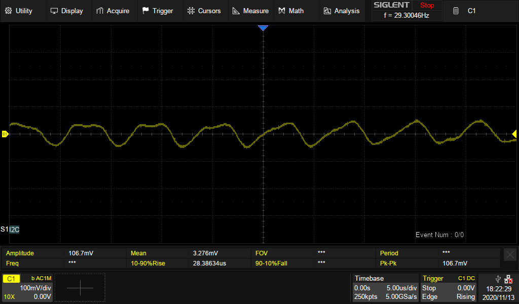
Input stage
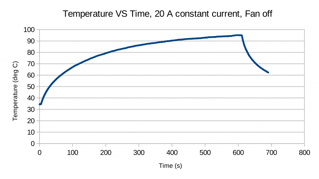
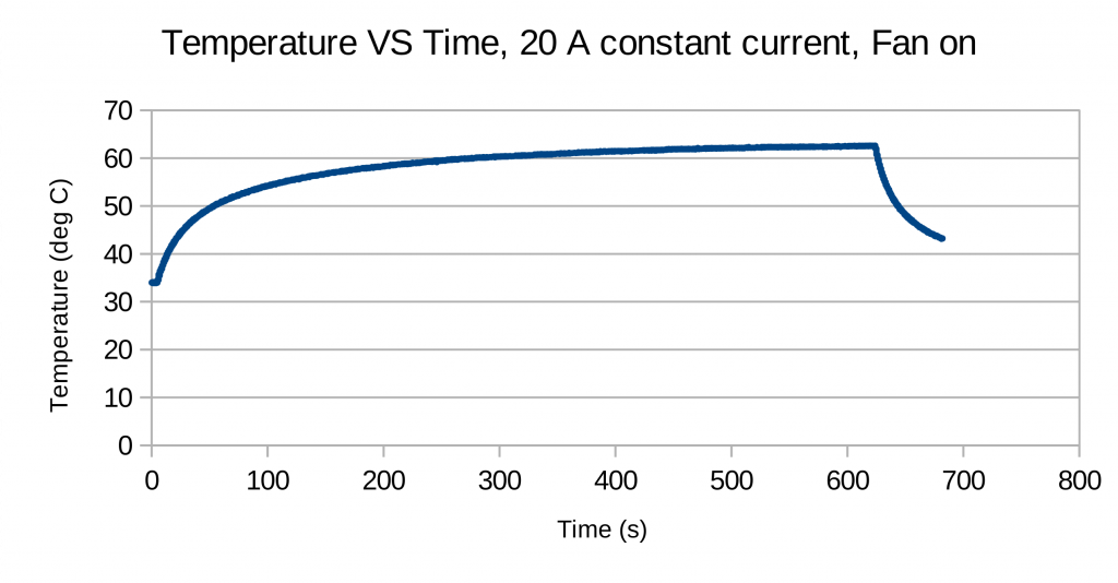
An experiment with a constant current load drawing 20 A from the bed connector with and without a 92 mm fan on top of the board for forced convection. The temperature measured was with the on board thermistor. Using a thermal camera, the temperature displayed matches well with the temperature reported by the camera. However, in Rev A2, this is not the hottest point on the board. The MOSFET controlling the bed seems to consistently get the highest temperature. The reason for this is probably due to a 3.3 V VGS.
Inrush current
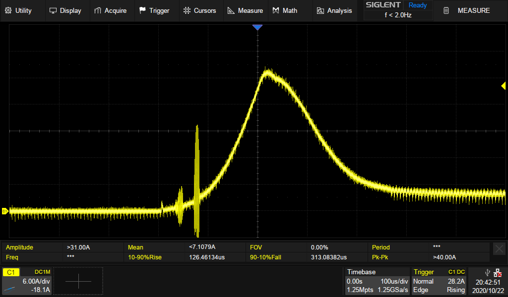
During turn on of the high power stage, there will be an inrush current to charge up the bank of capacitors present on the board.
If no loads are turned on, the inrush current reaches 31 A at peak. This is important to consider when setting the current limit with device tree.
Temperature low pass filter
A Low pass filter has been added on each of the temperature input channels. The cut-off frequency is below what my oscilloscope can handle, but a plot in the time domain verifies a 7 Hz -3dB point.
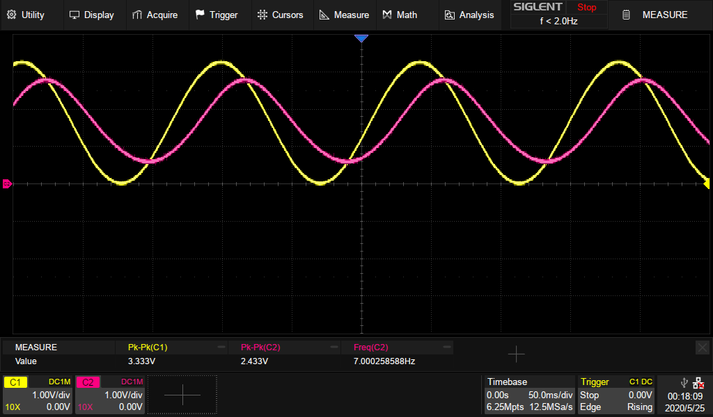
ADC offset and gain measurements
To measure the ADC offset error, measure the voltage on the uC input pin and record when the transition from 0 to 1 occurs. It should occur at 0.5 LSB = 3.3/4096/2 = 0.4028 mV. Offset: 55.35 mV - 0.4028 mV = 54.95 mV
FAQ
Q: Where can I ask for help?
A: You can join the Discord: https://discord.gg/bCnp9H5SB5
Q: What comes in the box with the Recore? Specifically, terminal connectors for power, etc?
A: It's only the board, no connectors at all. There will be a bag of connectors available to purchase eventually, but for now you will have to supply your own.
Q: What's the maximum current draw for heat bed?
A: This has been tested up to 20 A
Q Why are there unused and unbroken out pins on the STM32 MCU?
A: The pins that are needed from the MCU have been routed out plus two pins available on an external header.
Q: I have a gadget that I want to connect with SPI. Is that possible?
A: There are 6 pins available from the main SoC that can be used for various things. There is no hardware SPI, but you can make a program that uses soft SPI. There is no dedicated I2C, but perhaps that would be a nice addition.
Q: What exactly is the role of the AR100 device?
A: The AR100 handles the fast realtime aspects, mainly the stepper motors
Q: What voltage fans are supported?
A: The same voltage as the input voltage, either 12 V or 24 V. You can experiment with PWM for running lower voltage fans on 24 V input.
Q: Where is the board layout file?
A: The Layout file will not be available. It is an "open schematic" board, not open source hardware
Q: Where are you shipping from?
A: Early prototypes (Rev A4) will be shipping from Norway. Eventually shipping will be from a warehouse in the US
Known Issues
Noisy thermocouple readings
Because the op-amp gain is programmable with a GPIO pin, the level is not pulled down hard enough, so noise is coupled into the gain of the op-amp.
Offset on thermistor readings
The TVS diodes have too high leakage current causing an offset on the readings at low temperatures.

